- 您现在的位置:买卖IC网 > Sheet目录624 > HWK60000 (Red Lion Controls)KIT BEZEL WITH PC BOARD & CABLE
�� �
�
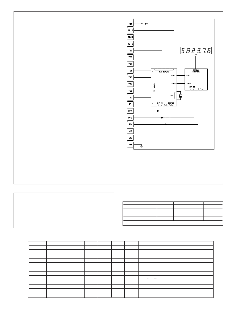
�DEVICE� CONNECTIONS�
�TB12� -� CMOS� *Pulsed� Pull-up� Latched� input.� When� input� is� connected� to�
�V� SS� ,� 8� seconds� is� added� to� the� total� time� base� period.� When� input� is�
�connected� to� V� DD� or� left� open,� no� time� is� added� to� the� total� time� base�
�period.�
�TB11� -� CMOS� *Pulsed� Pull-up� Latched� input.� Adds� 4� seconds� to� the� total�
�time� base� period� when� input� is� connected� to� V� SS� .�
�TB10� -� CMOS� *Pulsed� Pull-up� Latched� input.� Adds� 2� seconds� to� the� total�
�time� base� period� when� input� is� connected� to� V� SS� .�
�TB9� -� CMOS� *Pulsed� Pull-up� Latched� input.� Adds� 1� second� to� the� total� time�
�base� period� when� input� is� connected� to� V� SS� .�
�TB8� -� CMOS� *Pulsed� Pull-up� Latched� input.� Adds� 1/2� second� to� the� total�
�time� base� period� when� input� is� connected� to� V� SS� .�
�TB7� -� CMOS� *Pulsed� Pull-up� Latched� input.� Adds� 1/4� second� to� the� total�
�time� base� period� when� input� is� connected� to� V� SS� .�
�TB6� -� CMOS� *Pulsed� Pull-up� Latched� input.� Adds� 1/8� second� to� the� total�
�time� base� period� when� input� is� connected� to� V� SS� .�
�TB5� -� CMOS� *Pulsed� Pull-up� Latched� input.� Adds� 1/16� second� to� the� total�
�time� base� period� when� input� is� connected� to� V� SS� .�
�TB4� -� CMOS� *Pulsed� Pull-up� Latched� input.� Adds� 1/32� second� to� the� total�
�time� base� period� when� input� is� connected� to� V� SS� .�
�TB3� -� CMOS� *Pulsed� Pull-up� Latched� input.� Adds� 1/64� second� to� the� total�
�time� base� period� when� input� is� connected� to� V� SS� .�
�TB2� -� CMOS� *Pulsed� Pull-up� Latched� input.� Adds� 1/128� second� to� the� total�
�time� base� period� when� input� is� connected� to� V� SS.�
�TB1� -� CMOS� *Pulsed� Pull-up� Latched� input.� Adds� 1/256� second� to� the� total�
�time� base� period� when� input� is� connected� to� V� SS.�
�DPA� -� CMOS� *Pulsed� Pull-up� Latched� input.� When� used� along� with� DPB,�
�selects� the� position� of� the� decimal� point.�
�DPB� -� CMOS� *Pulsed� Pull-up� Latched� input.� When� used� along� with� DPA,�
�selects� the� position� of� the� decimal� point.�
�F.D.� -� CMOS� *Pulsed� Pull-up� Latched� input.� When� input� is� connected� to� V� SS� ,�
�Frequency� Doubling� is� disabled.� When� input� is� connected� to� V� DD� or� left�
�open,� Frequency� Doubling� is� enabled.�
�M.R.� -� CMOS� Internally� Pulled-up� input.� When� input� is� connected� to� V� SS� ,�
�Master� Reset� will� terminate� the� present� time� base� period.� When� MR� is�
�allowed� to� go� high,� the� next� time� base� period� will� begin.� In� normal� use,�
�MR� is� connected� to� V� DD� or� left� open.� Note� that� this� is� not� a� Pulsed� Pull-�
�up� Latched� input.�
�*� See� section� on� “Pulsed� Pull-Up� Latched� Inputs”� for� more� information� .�
�Note:� For� maximum� noise� immunity� ,� connect� all� TB� inputs� to� either� V� DD� or�
�V� SS� ,� whichever� is� appropriate.� Inputs� left� open� may� change� states� in� some�
�noisey� environments.�
�BLOCK� DIAGRAM�
�SIG.� -� CMOS� Schmidt� trigger� input.� Counter� chip� increments� on� the� falling�
�edge� of� the� Signal� input� when� F.D.� is� connected� to� V� SS� (disabled).� Counter�
�chip� increments� on� both� rising� and� falling� edges� of� the� Signal� input� when�
�F.D.� is� connected� to� V� DD� or� left� open� (enabled).�
�V� DD� -� +2.5� to� 6.0� VDC� Supply�
�V� SS� -� Common� for� D.C.� Supply� and� Inputs.�
�C�
�C�
�CAUTION�
�This� device� contains� CMOS� circuitry� which� requires� special� anti-static�
�handling� to� the� same� degree� required� by� standard� CMOS� integrated� circuits.�
�Units� should� be� stored� in� the� conductive� packaging� used� to� ship� the� devices.�
�Containers� should� be� opened� and� units� handled� only� on� a� conductive� table�
�top� by� personnel� wearing� wrist-strap� grounding� equipment.� These� devices�
�have� the� same� protection� circuits� as� standard� CMOS� devices� to� prevent�
�MAXIMUM� RATINGS� (VOLTAGE� REF.� TO� V� SS� )�
�RATING� SYMBOL� VALUE�
�DC� Supply� Voltage� V� DD� -0.5� to� +6.5�
�Input� Voltage,� All� Inputs� V� I� -0.5� to� (V� DD� +0.5)�
�Operating� Temperature� *� T� A� -35� to� +85�
�Storage� Temperature� T� STG� -35� to� +85�
�UNIT�
�VDC�
�VDC�
�o�
�o�
�damage� to� inputs� due� to� nominal� over-voltage.�
�*� Extended� high� and� low� temperature� ranges� available,� consult� factory.�
�ELECTRICAL� CHARACTERISTICS� V� DD� =� 5� V� ±10%� UNLESS� OTHERWISE� SPECIFIED�
�SYMBOL�
�V� DD�
�I� DD�
�I� DDQ�
�V� SIH�
�V� SIL�
�V� IH�
�V� IL�
�PARAMETER�
�Supply� Voltage�
�Supply� Current�
�Supply� Current�
�Input� High� Voltage�
�Input� Low� Voltage�
�Input� High� Voltage�
�Input� Low� Voltage�
�MIN.�
�2.5�
�3.9�
�TYP.�
�3.0�
�0.9�
�2.2�
�2.1�
�MAX.�
�6.0�
�55�
�45�
�0.5�
�UNIT�
�VDC�
�μA�
�μA�
�VDC�
�VDC�
�VDC�
�VDC�
�TEST� CONDITION�
�10� KHz� signal,� 1� second� time� base.� All� other� inputs� high.�
�1� second� time� base.� All� other� inputs� high.�
�Signal� input� only.�
�Signal� input� only.�
�All� other� inputs.�
�All� other� inputs.�
�I� SIL�
�I� IH�
�fc�
�R� PU�
�T� ACC�
�Input� Leakage�
�Input� High� Current� (source)�
�Signal� Frequency�
�Pull� Up� Resistance�
�Time� Base� Accuracy�
�50�
�0.05�
�0.01�
�50�
�0.1�
�200�
�500�
�μA�
�μA�
�K� W�
�%�
�V� DD� >� V� IN� >� V� SS� Signal� input� only.�
�All� other� inputs.�
�KHz�
�All� pull-up� inputs.�
�All� time� ranges.�
�2�
�发布紧急采购,3分钟左右您将得到回复。
相关PDF资料
HWK70000
CABLE ASSEM FOR MDM SERIES
IF-30-56
XFRMR 115/230V 28V 1.1A 30VA PCB
IL-20-0001
IL5 PULSE TRANSFORMER THT 0.25A
ILR-11-0003
ILR3 IMPULSTRAFO KONVENTIONELL
IS-1000
TRANSFORMER ISOLATION 1000W
IS-250
TRANSFORMER ISOLATION 250W
IS-500
TRANSFORMER ISOLATION 500W
IS1000HG
TRANSF ISO 1000W 4OUT HOSP GRADE
相关代理商/技术参数
HWK6M6
制造商:Hubbell Wiring Device-Kellems 功能描述:CAB, ACCESS,QUADCAB,MTG RAIL KT,M6,2'H
HWK70000
功能描述:CABLE ASSEM FOR MDM SERIES RoHS:是 类别:工业控制,仪表 >> 配件 系列:* 标准包装:1 系列:Aero-Motive® 130117 附件类型:拖车带 适用于相关产品:标准盒式跟踪系统 其它名称:WM6183
HWK9M6
制造商:Hubbell Wiring Device-Kellems 功能描述:CAB, ACCESS,QUADCAB,MTG RAIL KT,M6,3'H
HWKF120
制造商:Hubbell Wiring Device-Kellems 功能描述:CAB, ACCESS,QUADCAB,FAN KT,120VAC
HWKF230
制造商:Hubbell Wiring Device-Kellems 功能描述:CAB, ACCESS,QUADCAB,FAN KT,230VAC
HWKFF
制造商:Hubbell Wiring Device-Kellems 功能描述:CAB, ACCESS,QUADCAB,FAN FILTER KT
HWKGT
制造商:Hubbell Wiring Device-Kellems 功能描述:CAB, ACCESS,QUADCAB,GASKET KT
HWL 160W
制造商:Osram Opto semiconductors 功能描述:Bulk